
I've built several projects based on LED matrices: my first one in 2021, and a redesign earlier in 2025 with a larger panel and slimmer enclosure. I've also gotten to spend lots of time fine-tuning the display UI as I learn more about icon design, balancing readability and "glanceability" with information density, and dealing with the unique constraints of a display with a 3mm pixel pitch.
Link to this section Motivation
While the hardware was a dramatic step up from my first iteration, I still thought there was room for improvement: more robust mounting of the encoder and the DC power jack, a slimmer construction that could fit closer to the wall, and simpler internal wiring. The obvious next step was a custom PCB. This project came at a time when I was hoping to get back into PCB design, so this seemed like the perfect opportunity!
At the same time, I had relatively recently started full-time work and wanted to add some decorations to my desk area. Since my previous builds had proven extremely useful at indicating bus times and bike availability, I figured that one on my work desk would be similarly useful! Of course, this one had slightly different requirements, so I ended up building a single board and two very different enclosures for it.
Link to this section PCB Design
The schematic of the board is very similar to that of the previous build, with a few changes:
- The Adafruit LED Matrix Bonnet was removed and its level shifting chips were placed directly onto the custom PCB
- An ADC and photoresistor were added to enable automatic brightness dimming (a substantial pain point on the previous version!)
- A USB-C port was added to the side of the board as an alternate power option, since using the DC jack on the bottom would prevent standing the display up on a table

The layout followed pretty naturally. I kept the board at 192mm wide to match either a 64-column 3mm-pitch display or a 32-column 6mm-pitch display, gave it rounded bottom corners to match the style of the previous build, and mounted the encoder at the center on one side.

Shameless plug: The renders in this section were made in my KiCAD SVG prettifier tool.
While I like the enclosed build in my apartment, I wanted to leave the option of doing a build with an exposed PCB. The components are all mounted towards the back, and the routing was mostly done only on the back side, leaving the front part of the board mostly empty on both the silkscreen and copper layers. I thought about putting some artwork or text on the silkscreen but couldn't think of a good way to make it look professional -- the usable space on the board is asymmetrical and interrupted by through-hole components.
In the end, I decided to put a repeating pattern in the copper layer of the board, then order it with OSHPark's After Dark colorway, which uses transparent soldermask to let the copper design shine through. I wanted an angular style to match the vibes of the rigid exposed pixel grid, but worried that an actual grid pattern could clash or appear misaligned. Thus, I chose a hexagonal pattern.

Building and importing this pattern turned into more of an adventure than I had predicted! The process I found is convoluted and by no means ideal. If this were something I was doing more often I would definitely design an automated tool for it, but as it stands, the best way I know to accomplish this is:
- Make your board in KiCAD.
- Draw a shape in Inkscape representing your edge cuts in KiCAD. Make sure the units match up!
- Under "Fill", choose a pattern you like and set the scaling appropriately.
- Export your KiCAD board as an SVG so you can use it as a reference. The menu option for this is Plot > SVG, then select F.Cu, then check to have Edge.Cuts plotted on all layers.
- Import your plotted SVG into Inkscape and line it up using your Edge.Cuts layer as a reference.
- Manually draw shapes on top of the pattern to mask off all of the areas you do not want to have your copper pattern. It is easiest to put these in a group. These can be as convoluted or basic as you like -- I mostly sketched rectangles over large components and traces.
- Select all of your mask shapes and your shape with the pattern and open the "Shape Builder" tool. Select the area(s) where you want the pattern to show (i.e., the areas without parts). You should be left with a shape matching your intended board, containing your pattern as a fill.
- Next you need to turn the pattern into a basic SVG path. The easiest way to do this is to export it as a PNG (make sure your DPI is 500ish), then re-import it and use the "Trace Bitmap" feature. Click "Update Preview", and if it looks good then "Apply."
- Export as yet another SVG. (Make your F.Cu traces hidden before exporting!)
- In KiCAD, Use File > Import > Graphics, select your layer (in our case F.Cu), then place it and manually line it up with your board!
At my girlfriend Mia's suggestion, I added a photoresistor and ADC to the circuit to implement automatic brightness control. I haven't gotten around to using this yet, mainly because the build at my work desk does not require it and the enclosure design of the one at home blocks outside light. In the future I think I could add a small hole to the bottom of the design which would let light into the enclosure but not be too visible.
Link to this section PCB Assembly
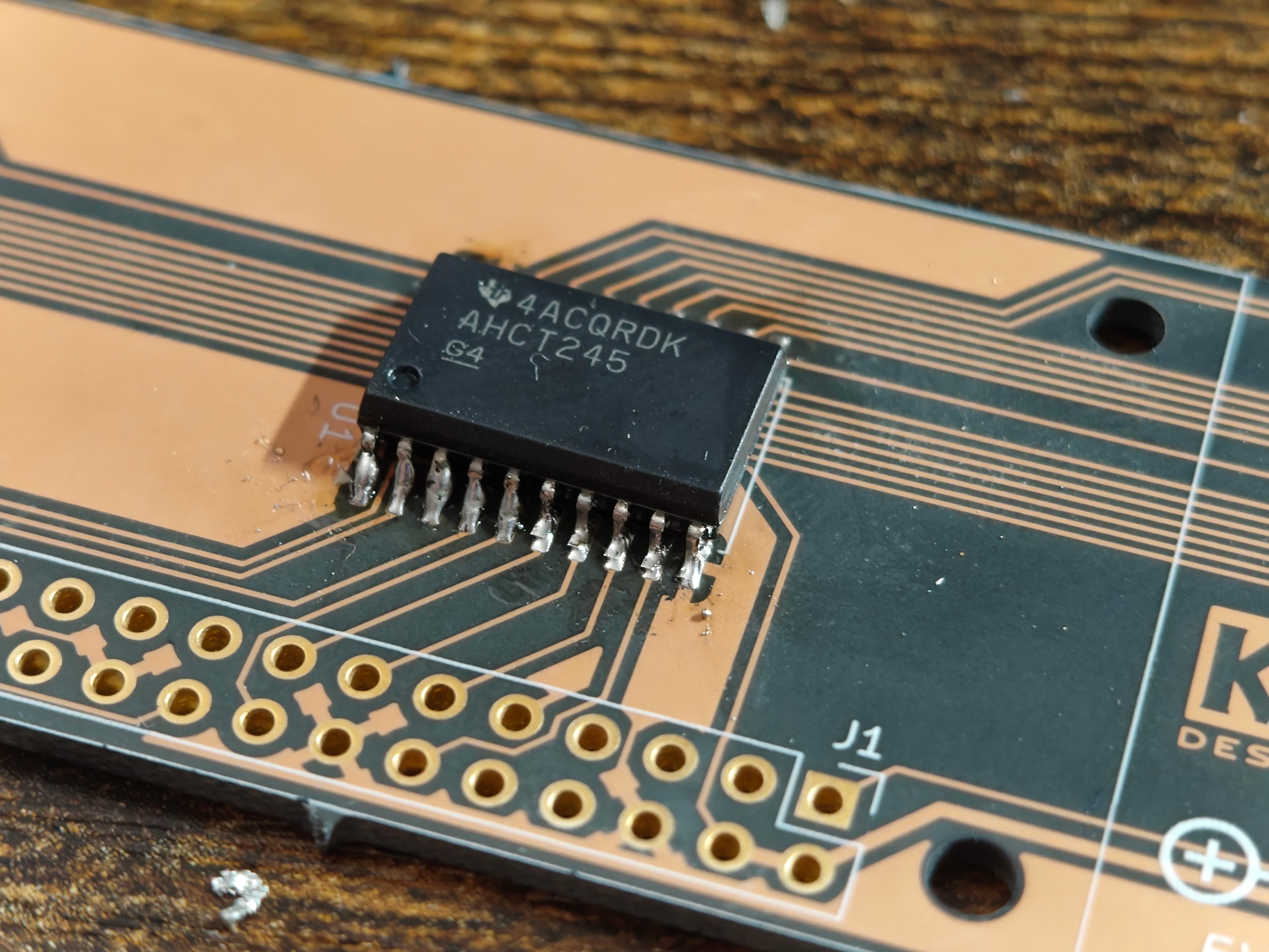
This was my first time doing surface-mount soldering! I kept the components manageable (SOIC chips and 0805 passives). Overall I found the experience much easier than I anticipated. Big thanks to Mia for giving very helpful advice throughout. Thankfully, the board worked on the first try!
Link to this section Enclosure
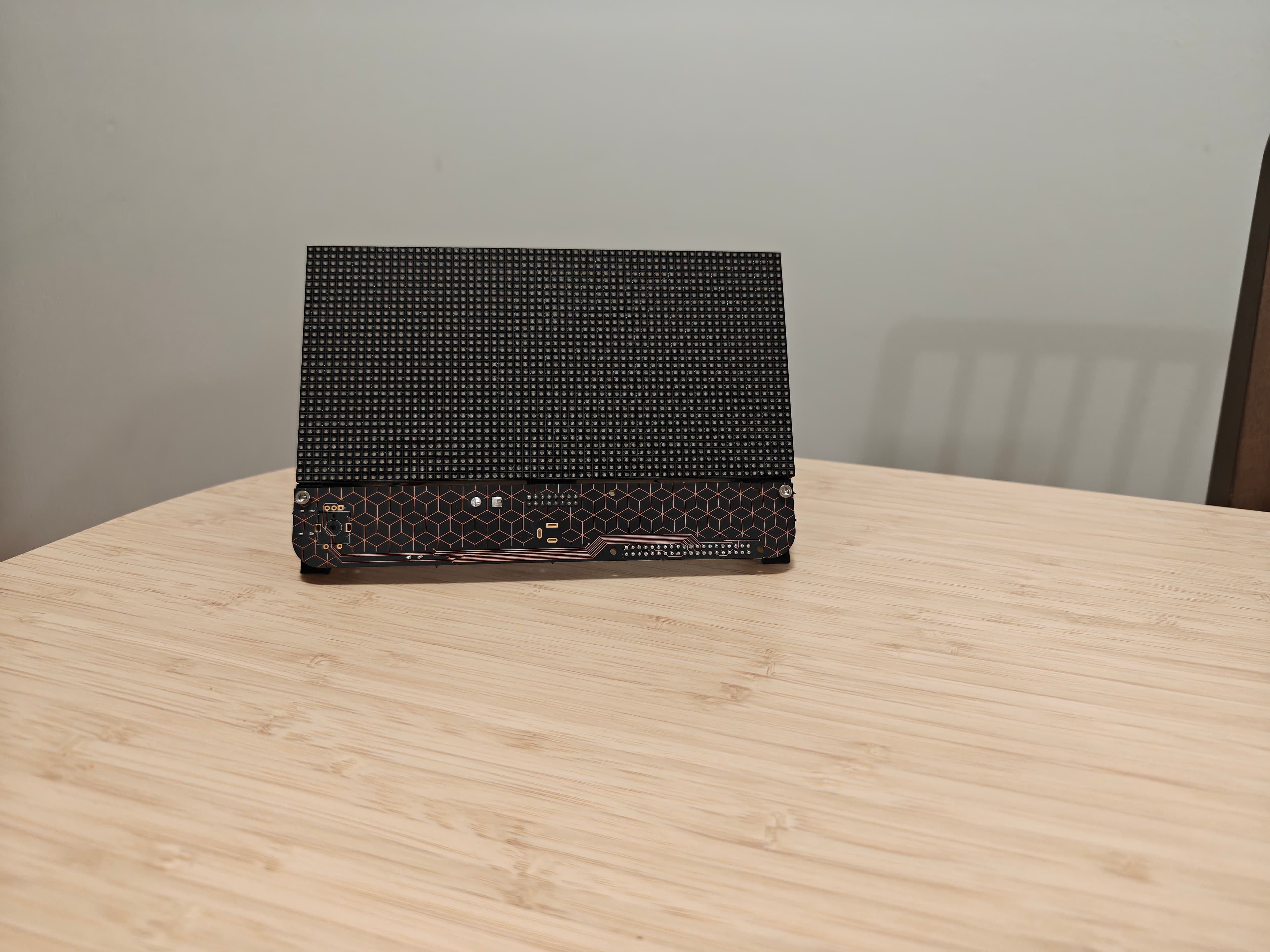
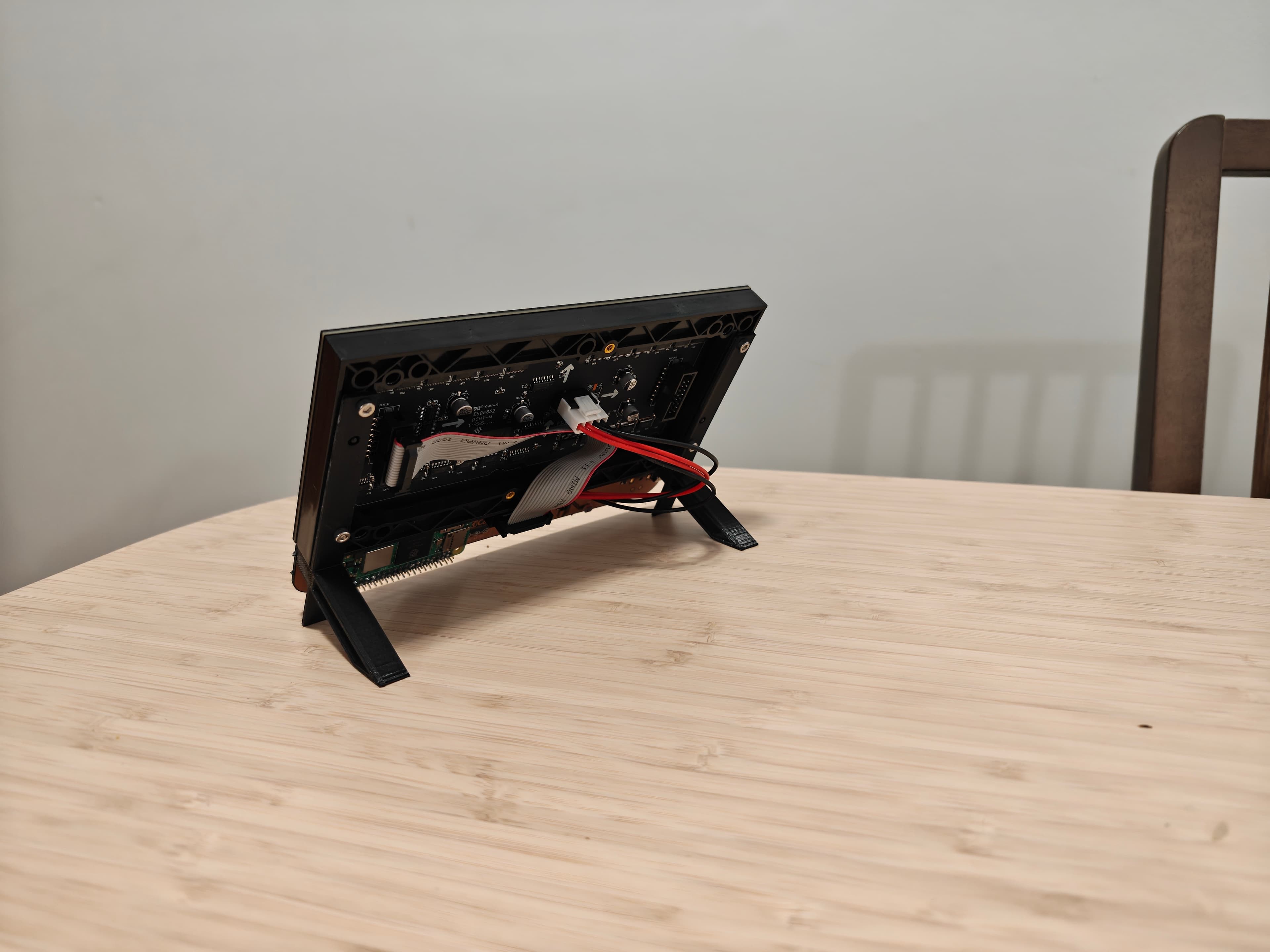
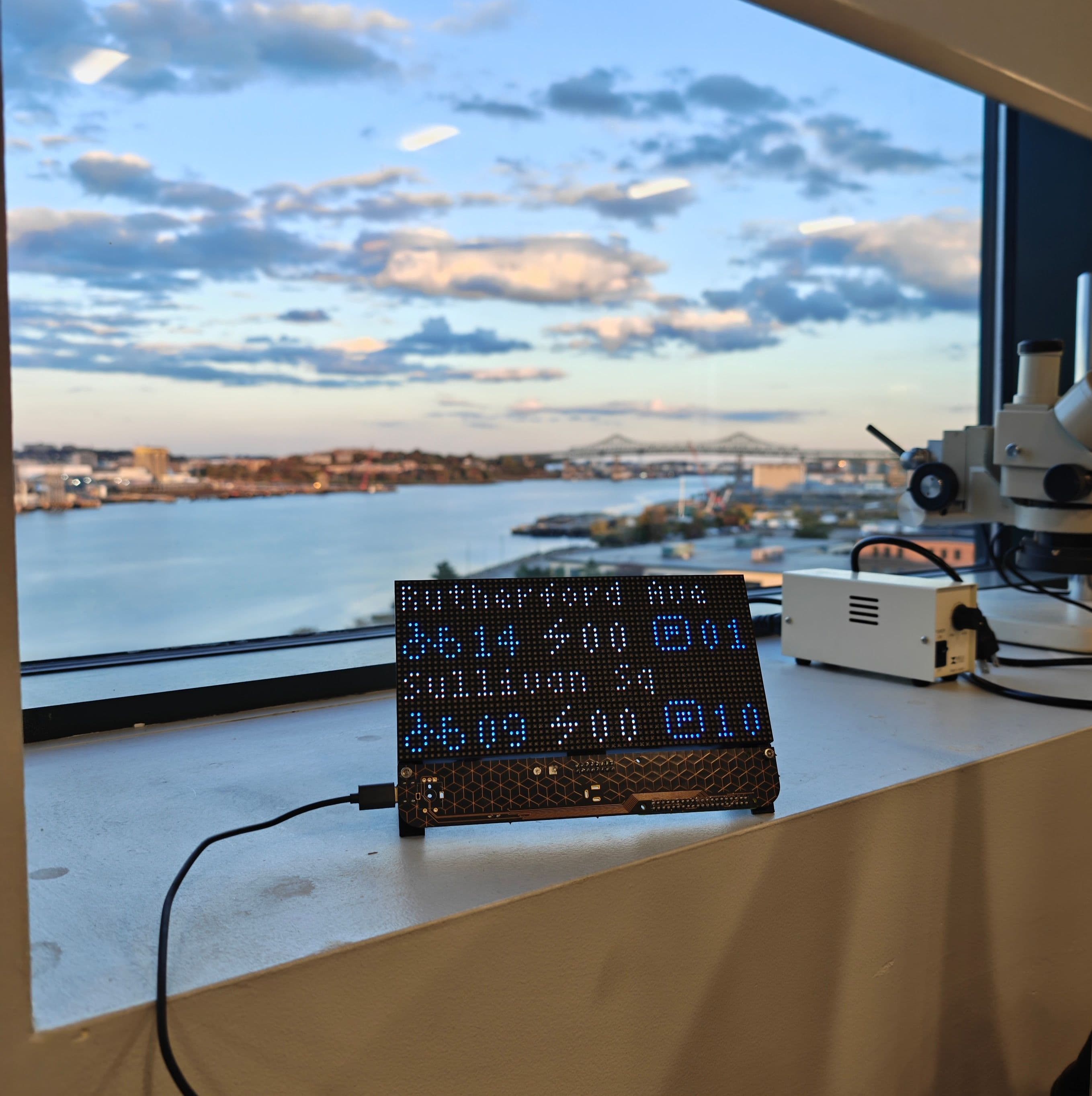
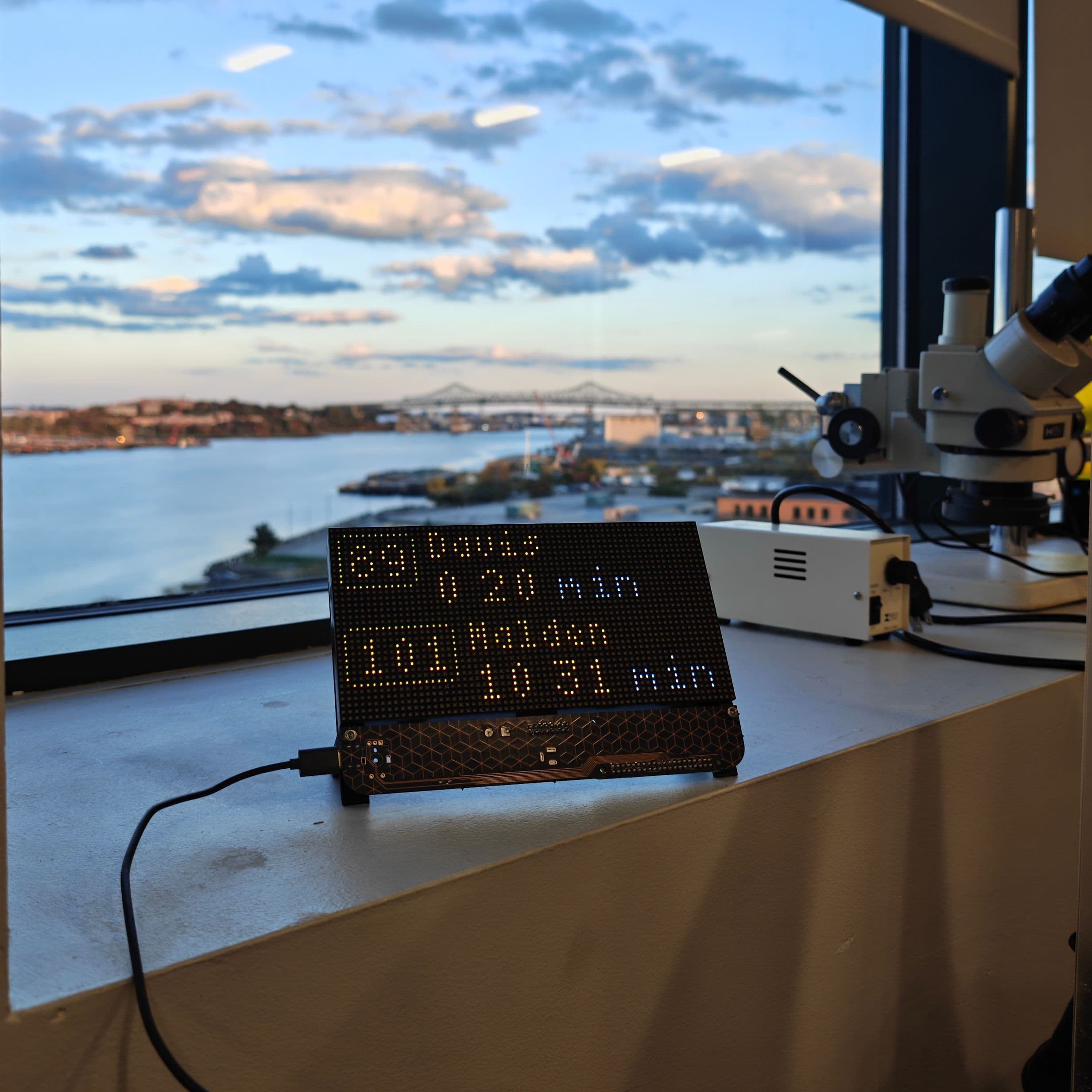
For the build sitting at my work desk, I wanted to build something that showed off the internals while still appearing sturdy and thoughtfully designed. I went with two small 3D-printed parts on opposite sides of the assembly which attach to both the PCB and the panel, allowing the device to be freestanding on a desk or table.
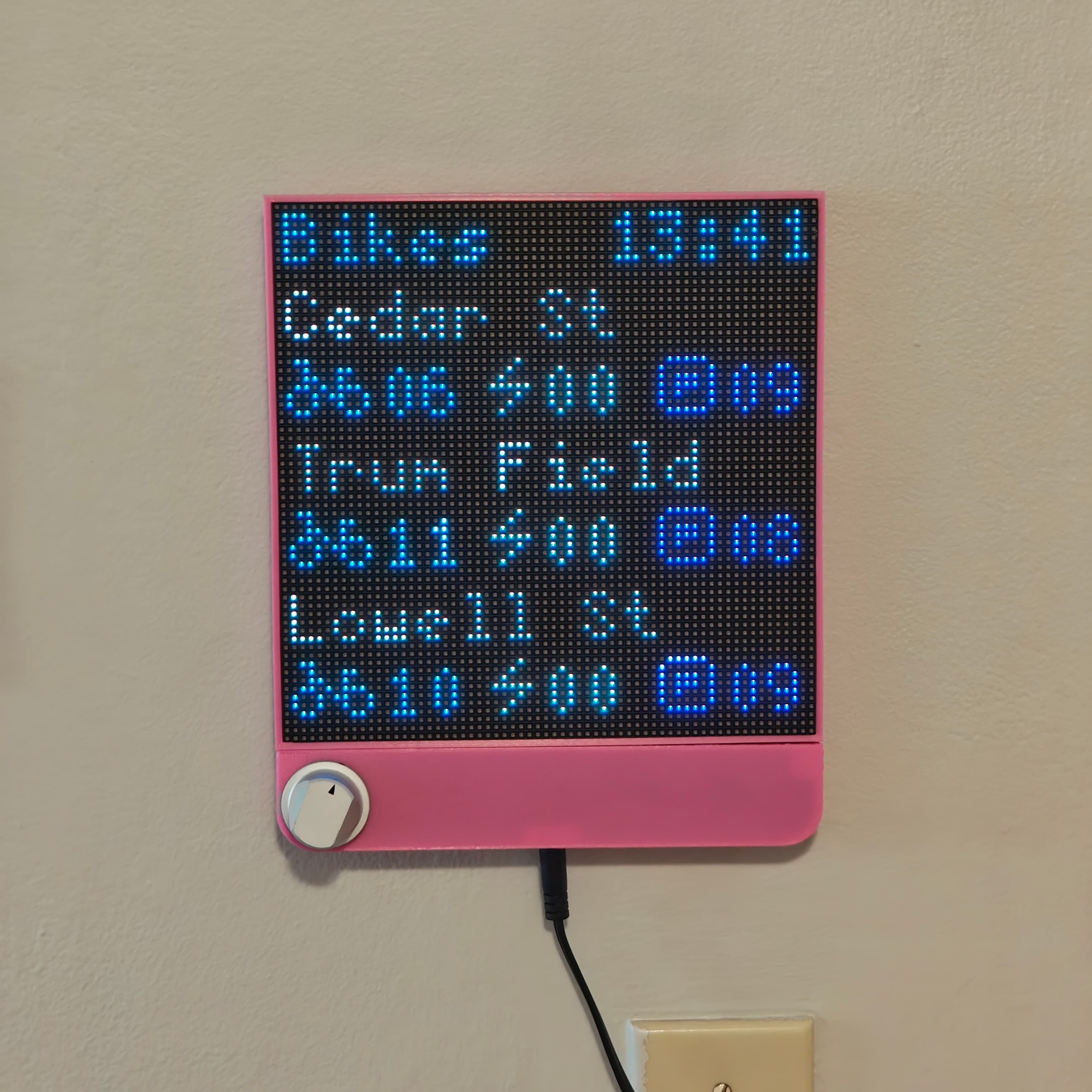
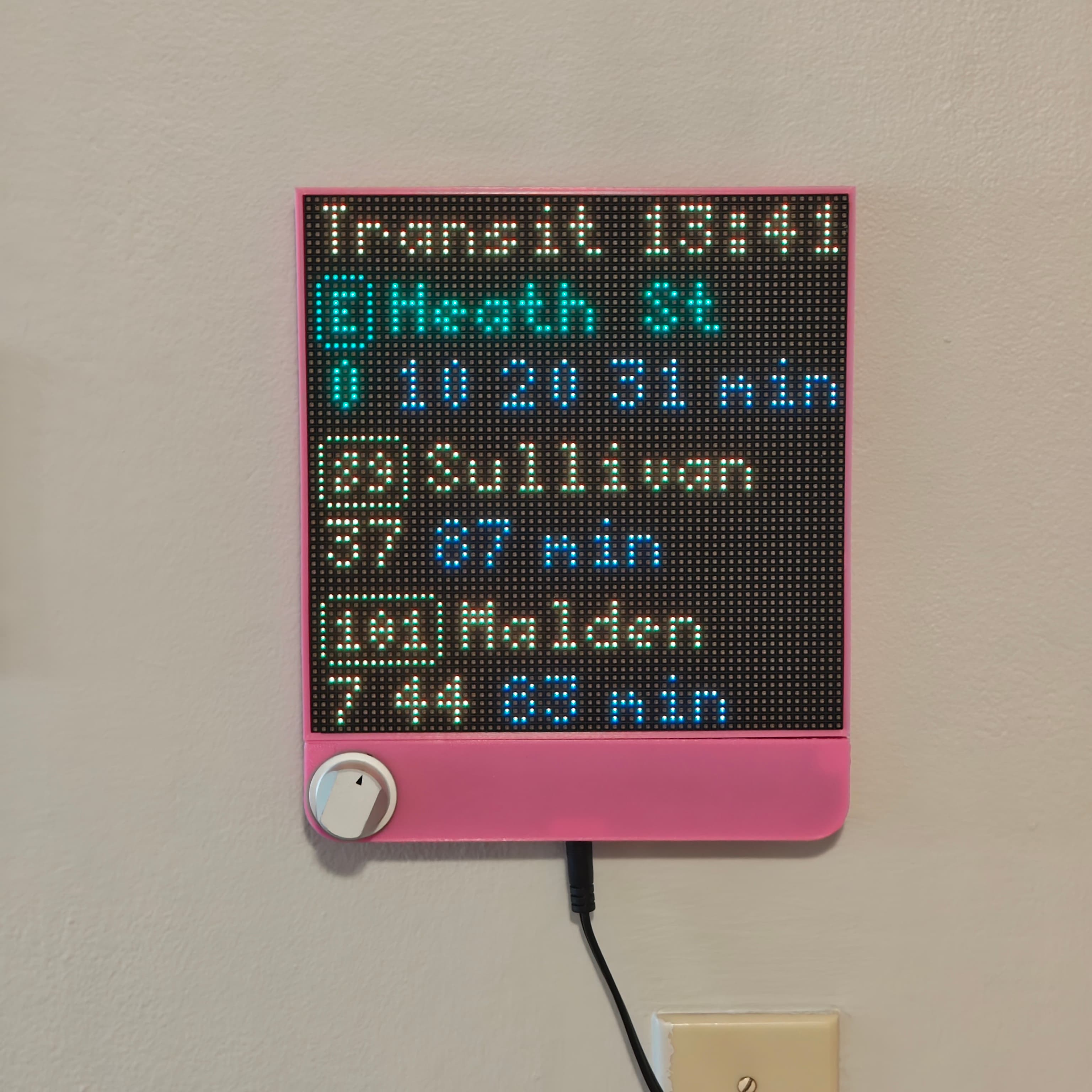
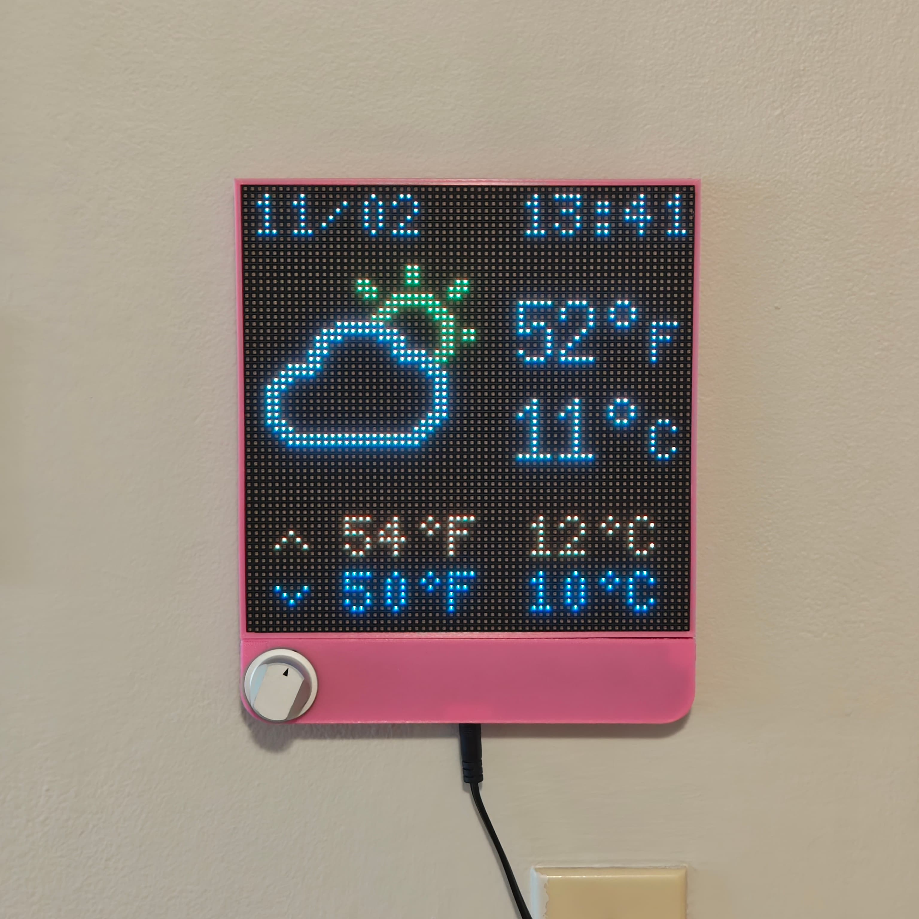
For the one in my apartment, I wanted to continue the theme of building something as unobtrusive as possible. Since the PCB was now the same width of the panel, if I wanted to enclose the PCB fully, the enclosure would also need to be a few millimeters wider than the panel. I took this opportunity to recess the panel into the enclosure, giving the system a much more polished look from the side view.
I am not super happy with the large gaps in the design caused by the imprecision of my 3D printer. I do like that 3D printing can give a brightly colored end result, and the form of the parts seems to lend itself well to a 3D-printed design over something like CNC milling. Perhaps I just need to get access to a better 3D printer.
The knob was given to me by a coworker who happened to be getting rid of it. It fits my encoder shaft perfectly! It is a bit taller than I would like but that is mostly a function of how much the shaft protrudes. In the future I will get a shorter encoder shaft or find a way to mount the encoder farther back. I unfortunately can't move the entire PCB back without increasing the thickness of the system because of the height of the 2x8 connector going to the LED panel.
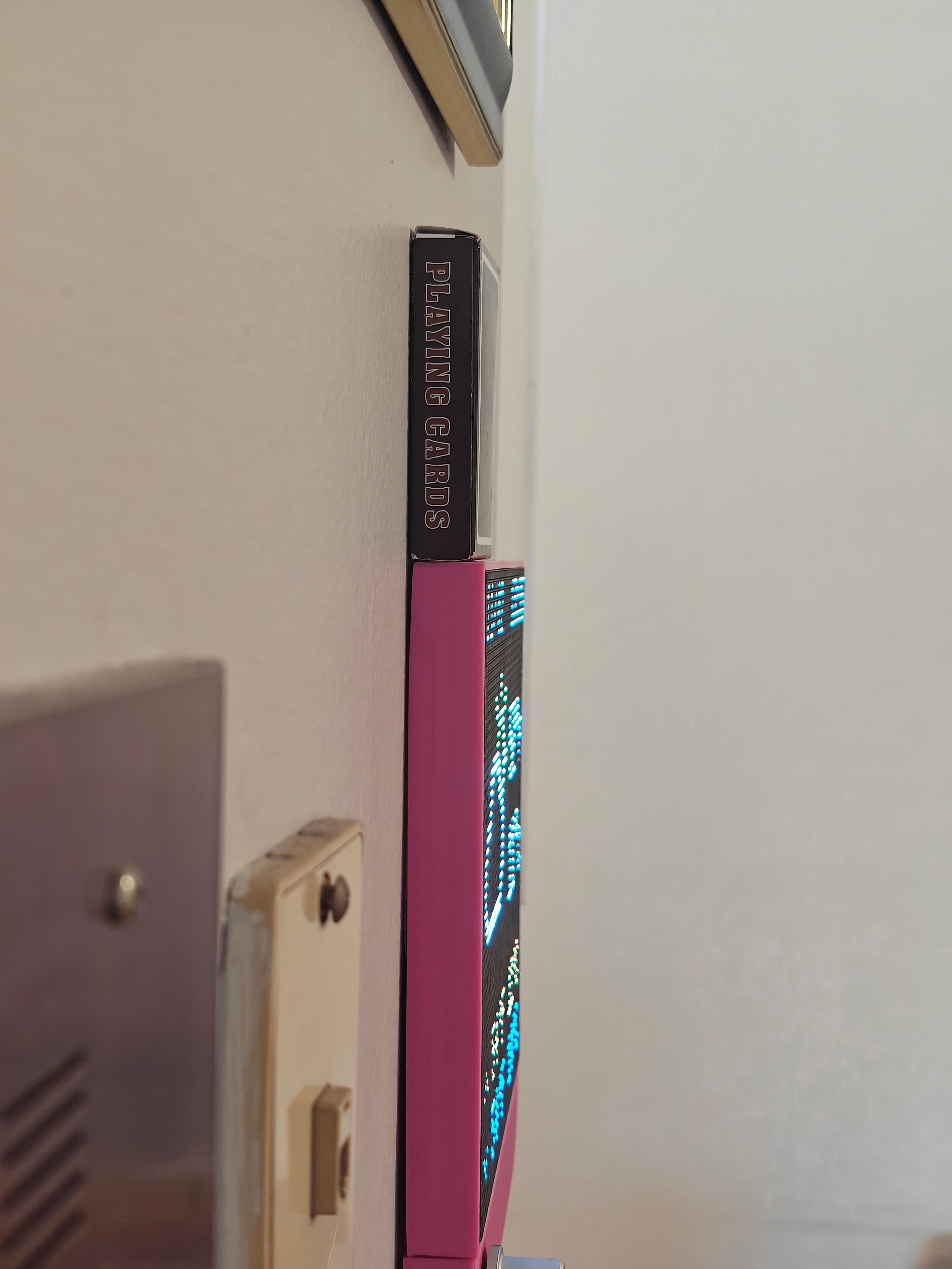
One thing I do love about the new design is that it sits dramatically closer to the wall, making it match the thickness of photos and artwork I have. Things have come a long way from the ~50mm thickness of the original version!
Link to this section Software
The largest changes on the software standpoint were extending the previous version to support multiple display sizes and moving a lot of the hardcoded logic (ZIP codes, etc) into a configuration file so my display at work could show different information to my display at home.
I hacked together a barely-working implementation to test the panel which Ava kindly refactored into something much nicer.
Link to this section Conclusion
I think time has shown that I'm unlikely to stop building this kind of display anytime soon. They serve a really interesting niche of a device that provides basic information at a glance without being obtrusive, and have a unique and interesting look.
I really enjoyed getting back into PCB design and finally conquering my fears regarding surface-mount work. I hadn't actually designed and gotten a board fabricated since I was in high school, more than 5 years ago! It was nice to exercise that skill again. SMT soldering, on the other hand, is something I had never attempted before, being scared off by my general clumsiness and the precision and tools often recommended for that kind of work. While I am very glad I bought flux at the recommendation of a friend, I found it to be smooth sailing even without new tips for my iron. Perhaps I'll invest in some better tools in the future.
I loved getting to design this iteration with a focus on making it easy to potentially build more in the future. The board came out quite nice, and while there are definitely some things I would change in the future (mostly relating to making the connectors protrude farther out of the case), I am overall quite happy with the results!
Throughout this process, several few people have told me that they would love to build something similar to this for their home. I've considered a few times trying to scale up production, but the parts cost (mostly the panel itself and the Raspberry Pi) makes the total cost of each unit pretty high. There are a few companies making something similar (Tidbyt and RideOnTime are the two I've seen), but they both use small panels in a thick enclosure style like I did in the first iteration of this project. I've grown to really appreciate the large 64x64 panel size as an option, a flat enclosure, and a design more focused on information density.
I don't want to start a business selling these or anything, but I could see myself creating better documentation of what hardware to buy, making the software easier to install and use, and organizing a group buy of boards and parts. Shoot me a message if that sounds interesting to you!